
THANK YOU FOR SUBSCRIBING


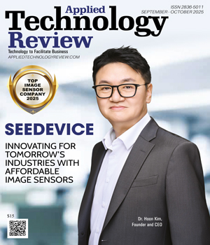
 Dr. Hoon Kim, Founder and CEO
While the benefits of this cutting-edge technology are undeniable, the high costs of development and implementation often put it out of reach for many industries, particularly smaller players or those with limited budgets.
SeeDevice Inc. is breaking this mold by blending advanced capabilities with affordability.
The company offers a sensor that detects a wide range of wavelengths using a unique, silicon-based CMOS process. The result is a game-changing SWIR solution that’s transforming sectors from agriculture to healthcare, gaming, and automotive, all without the high costs typically associated with such advancements.
A VISION THAT BEGAN ALMOST A DECADE AGO
SeeDevice Inc. was founded nearly a decade ago by Dr. Hoon Kim, whose deep experience in technology and research laid the groundwork for the company’s innovation.
Before establishing SeeDevice, Dr. Kim served as a professor at the University of Utah and as the director of Nano Quantum Devices Center at KETI (Korea Electronics Technology Institute). With a strong academic background and a proven track record in technological development, Dr. Kim’s move into the private sector was driven by his desire to create practical, scalable solutions for industries in need of advanced imaging technologies.
His journey began with the aim of bridging the gap between high-performance imaging sensors and the cost-prohibitive technologies that were limiting their widespread adoption. Prior to SeeDevice’s inception, most image sensors capable of detecting wavelengths across the electromagnetic spectrum relied on rare, expensive materials such as indium gallium arsenide or germanium. These materials were costly and difficult to scale, limiting their availability and affordability for many applications.
Dr. Kim’s breakthrough came when he developed a patented technology based on pure silicon. By incorporating the quantum tunnelling effect and plasmonic field enhancement into his design, he was able to create a CMOS image sensor capable of detecting wavelengths from the X-Ray range all the way to short-wave infrared. This groundbreaking sensor has since set SeeDevice apart from competitors and opened new possibilities in imaging.
QUANTUM-DRIVEN INNOVATION
SeeDevice’s ability to detect such a broad spectrum of wavelengths with precision and affordability makes it unique. The company’s sensors are based on a quantum-driven innovation that combines two fundamental concepts: the quantum tunnelling effect and plasmonic field enhancement.
 At its core, the quantum tunnelling effect allows the sensor to pass through energy barriers that would normally be insurmountable for conventional sensors. This enables it to detect wavelengths from the X-Ray spectrum to the short-wave infrared range, providing a far wider range than any other CMOS sensor technology. Additionally, plasmonic field enhancement improves the sensor’s ability to detect and amplify light signals, enhancing overall sensitivity and efficiency.
SeeDevice’s CMOS image sensors are built entirely with silicon, making them both affordable and easy to manufacture at scale. This breakthrough in manufacturing enables the company to offer a powerful sensor at a fraction of the price of competing products. Dr. Kim, Founder & CEO at SeeDevice, explains the significance of the technology:
“Our quantum-based CMOS image sensor technology enables us to achieve capabilities previously reserved for sensors that used expensive, exotic materials. What we’ve done is take that high performance and make it scalable, affordable, and easy to mass-produce.”
FROM AGRICULTURE TO GAMING
SeeDevice’s SWIR technology is already making a significant impact across various industries. One of the company’s most exciting collaborations is with John Deere, the world’s leading manufacturer of agricultural machinery. SeeDevice has collaborated to integrate its image sensors into John Deere’s equipment, helping farmers monitor yield level in grain cart day or night, even in harsh environment, maintain crop health, and detect defects in real time with remarkable accuracy. This collaboration has the potential to improve crop yields, optimize farming practices, and reduce waste—ultimately revolutionizing precision farming.
In addition to agriculture, SeeDevice is also working with a prominent gaming device company to integrate its sensors into the next generation of gaming consoles. This application demonstrates the versatility of SeeDevice’s SWIR technology, which can be seamlessly adapted for use in consumer electronics. By embedding advanced imaging capabilities into gaming consoles, SeeDevice is helping to deliver new experiences to players while keeping production costs low.
One of the most compelling applications of SeeDevice’s SWIR technology is in healthcare—specifically in non-invasive glucose monitoring devices. Diabetes affects millions of people worldwide, and current glucose monitoring methods require painful finger pricks. SeeDevice’s sensors enable a non-invasive solution, allowing patients to place their fingers on a sensor to measure glucose levels without the need for needles. This solution is not only more convenient for users but also significantly more affordable than existing alternatives.
Furthermore, SeeDevice is targeting the automotive industry, particularly the rapidly growing market for autonomous vehicles. Traditional lidar systems, which are essential for self-driving cars, are costly and complicated to manufacture. SeeDevice’s sensors, however, offer a more cost-effective solution by providing accurate, long-range imaging. This has the potential to make autonomous vehicles more accessible and affordable, bringing self-driving technology to the mass market.
AFFORDABLE, SCALABLE, AND EFFICIENT
One of the defining features of SeeDevice’s SWIR technology is its affordability. While many advanced image sensors rely on rare materials that make them prohibitively expensive, SeeDevice’s sensors are made with pure silicon, allowing them to be produced at a fraction of the cost. With a production cost about ten dollars per chip, these image sensors offer significant savings compared to traditional alternatives, which can cost thousands of dollars per unit.
This affordability is paired with the company’s ability to mass-produce its sensors at a high yield rate. Many competitors face challenges in scaling their production due to low yields, which can lead to delays and increased prices. SeeDevice, on the other hand, has mastered the art of high-yield, mass production, ensuring it can meet global demand while keeping costs low.
From medical devices to consumer electronics, SeeDevice’s sensors are positioned to disrupt a variety of sectors, making advanced imaging technology accessible to businesses that may have previously been priced out of the market.
A BRIGHT FUTURE AHEAD
SeeDevice is preparing for a major leap in its growth trajectory. The company is set to begin mass production of its image sensors by the end of this year or early next year, marking a significant milestone in its journey. As the technology moves from prototype to full-scale manufacturing, SeeDevice plans to expand its applications to other industries, further solidifying its position as a leader in the image sensor space.
“We’re just scratching the surface of what’s possible with our technology,” Mr. Sean Oh, Senior Vice President & Chief Marketing Office at SeeDevice notes. “Over the next 18 to 24 months, we expect to see our technology adopted across a wide range of industries. The future is incredibly bright for SeeDevice.”
The company’s current focus is on refining its sensors for applications in automotive systems, healthcare, gaming, and agriculture, but it is also exploring new use cases. SeeDevice’s ultimate goal is to make high-performance, affordable SWIR sensors a standard feature in a variety of devices, helping businesses across different sectors improve their capabilities without incurring prohibitive costs.
SeeDevice’s SWIR technology is already making a significant impact across various industries. One of the company’s most exciting collaborations is with John Deere, the world’s leading manufacturer of agricultural machinery. SeeDevice has collaborated to integrate its image sensors into John Deere’s equipment, helping farmers monitor yield level in grain cart day or night, even in harsh environment, maintain crop health, and detect defects in real time with remarkable accuracy. This collaboration has the potential to improve crop yields, optimize farming practices, and reduce waste—ultimately revolutionizing precision farming.
In addition to agriculture, SeeDevice is also working with a prominent gaming device company to integrate its sensors into the next generation of gaming consoles. This application demonstrates the versatility of SeeDevice’s SWIR technology, which can be seamlessly adapted for use in consumer electronics. By embedding advanced imaging capabilities into gaming consoles, SeeDevice is helping to deliver new experiences to players while keeping production costs low.
-
Our quantum-based CMOS image sensor technology enables us to achieve capabilities previously reserved for sensors that used expensive, exotic materials. What we’ve done is take that high performance and make it scalable, affordable, and easy to mass-produce.
One of the most compelling applications of SeeDevice’s SWIR technology is in healthcare—specifically in non-invasive glucose monitoring devices. Diabetes affects millions of people worldwide, and current glucose monitoring methods require painful finger pricks. SeeDevice’s sensors enable a non-invasive solution, allowing patients to place their fingers on a sensor to measure glucose levels without the need for needles. This solution is not only more convenient for users but also significantly more affordable than existing alternatives.
Furthermore, SeeDevice is targeting the automotive industry, particularly the rapidly growing market for autonomous vehicles. Traditional lidar systems, which are essential for self-driving cars, are costly and complicated to manufacture. SeeDevice’s sensors, however, offer a more cost-effective solution by providing accurate, long-range imaging. This has the potential to make autonomous vehicles more accessible and affordable, bringing self-driving technology to the mass market.
AFFORDABLE, SCALABLE, AND EFFICIENT
One of the defining features of SeeDevice’s SWIR technology is its affordability. While many advanced image sensors rely on rare materials that make them prohibitively expensive, SeeDevice’s sensors are made with pure silicon, allowing them to be produced at a fraction of the cost. With a production cost about ten dollars per chip, these image sensors offer significant savings compared to traditional alternatives, which can cost thousands of dollars per unit.
This affordability is paired with the company’s ability to mass-produce its sensors at a high yield rate. Many competitors face challenges in scaling their production due to low yields, which can lead to delays and increased prices. SeeDevice, on the other hand, has mastered the art of high-yield, mass production, ensuring it can meet global demand while keeping costs low.
From medical devices to consumer electronics, SeeDevice’s sensors are positioned to disrupt a variety of sectors, making advanced imaging technology accessible to businesses that may have previously been priced out of the market.
A BRIGHT FUTURE AHEAD
SeeDevice is preparing for a major leap in its growth trajectory. The company is set to begin mass production of its image sensors by the end of this year or early next year, marking a significant milestone in its journey. As the technology moves from prototype to full-scale manufacturing, SeeDevice plans to expand its applications to other industries, further solidifying its position as a leader in the image sensor space.
“We’re just scratching the surface of what’s possible with our technology,” Mr. Sean Oh, Senior Vice President & Chief Marketing Office at SeeDevice notes. “Over the next 18 to 24 months, we expect to see our technology adopted across a wide range of industries. The future is incredibly bright for SeeDevice.”
The company’s current focus is on refining its sensors for applications in automotive systems, healthcare, gaming, and agriculture, but it is also exploring new use cases. SeeDevice’s ultimate goal is to make high-performance, affordable SWIR sensors a standard feature in a variety of devices, helping businesses across different sectors improve their capabilities without incurring prohibitive costs.
Expanding the Economics and Reach of Advanced Image Sensing
Image sensors sit at the center of modern electronics manufacturing, underpinning applications that range from industrial automation to medical diagnostics and intelligent vehicles. Executive teams evaluating next-generation sensing technologies confront a persistent constraint: performance beyond the visible spectrum typically carries a sharp cost premium and supply limitations. Sensors capable of detecting shortwave infrared or adjacent bands have relied on exotic materials such as indium gallium arsenide or germanium, which introduce fabrication complexity, limited yields and price points that confine adoption to niche deployments.
Manufacturing scale and bill-of-material discipline now shape board-level decisions as much as technical specifications. When a single chip can cost thousands of dollars and production yields remain constrained, downstream system design is forced into compromise. Product roadmaps slow, integration remains selective and emerging use cases never move beyond pilot stage. Executives therefore look for sensing platforms that extend spectral capability without breaking semiconductor manufacturing logic.
Three themes consistently determine long-term viability. The first is material strategy. Solutions that depend on nonstandard substrates or hybrid assemblies often struggle to achieve highvolume repeatability. Pure silicon compatibility, by contrast, aligns with established CMOS fabrication ecosystems, allowing companies to leverage existing foundry infrastructure and quality control regimes. The second theme is unit economics at scale. A design that can be manufactured at a fraction of prevailing market prices reshapes total system architecture, enabling multiple sensors per device rather than rationed placement. The third theme is cross-industry applicability. A sensor platform that supports agricultural machinery, medical monitoring, automotive perception and consumer electronics reduces concentration risk and signals architectural flexibility rather than single-vertical dependence.
Recent technical advances indicate that broader spectral detection need not require exotic materials. A silicon-based CMOS image sensor architecture incorporating quantum tunneling effects through plasmonic structures has demonstrated detection spanning from X-ray to shortwave infrared ranges. This approach departs from conventional assumptions that wide-spectrum sensing demands compound semiconductors. By embedding the necessary physics directly within a silicon process, it narrows the gap between advanced functionality and mass manufacturability.
Cost implications follow directly from that shift. Competing sensors using alternative materials have been associated with perchip prices in the thousands of dollars and constrained yields. A silicon-based implementation capable of mass production at fewer than ten dollars per chip alters the economic calculus. Lower unit cost supports redundancy, distributed sensing arrays and integration into mid-market products rather than only flagship platforms. High-yield manufacturing further addresses supply stability, a recurring concern in semiconductor procurement cycles.
Application breadth reinforces strategic relevance. Siliconbased wide-spectrum sensors are under development for integration into gaming hardware, agricultural equipment and noninvasive health monitoring devices, including glucose, blood pressure, heart rate and oxygen measurement. Automotive perception systems represent another frontier, where replacing expensive LIDAR configurations with camera-based alternatives could reduce system cost and accelerate adoption of driverassistance and autonomous capabilities. Such diversity signals architectural adaptability rather than a single-use breakthrough.
Within this landscape, SeeDevice represents a focused embodiment of these principles. Founded by a technologist who has developed the underlying physics over several decades, it has built a pure silicon CMOS image sensor capable of detecting across a broad spectral range while maintaining low production cost. Its emphasis on mass production, yield stability and crosssector deployment aligns closely with executive priorities in semiconductor and electronics manufacturing. For organizations intent on expanding spectral performance without inheriting material or supply risk, SeeDevice stands out as a disciplined and economically coherent choice.
...Read more
|
|

SeeDevice
Company
SeeDevice
Management
Dr. Hoon Kim, Founder and CEO
Description
SeeDevice Inc. is on the cutting edge of imaging technology, offering solutions that are both advanced and affordable. By leveraging a patented CMOS image sensor technology based on pure silicon and quantum effects, SeeDevice is setting a new standard for what’s possible in the world of imaging.

Copyright © 2026 Applied Technology Review.All Rights Reserved
Top
