
THANK YOU FOR SUBSCRIBING

Technology to Facilitate Business
× 
Applied Technology Review Weekly Brief
Be first to read the latest tech news, Industry Leader's Insights, and CIO interviews of medium and large enterprises exclusively from Applied Technology Review
Applied Technology Review: Specials Magazine

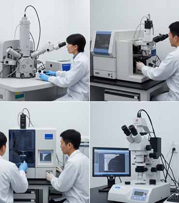
In controlled lab environments, achieving particle measurement precision is rarely the issue. But outside the lab, where temperature, humidity and flow dynamics can shift without warning, particle behavior becomes less predictable, and the true resilience of a measurement system is tested. Even the slightest misread in nanoparticle size distribution or aerosol concentration under fluctuating environmental conditions can lead to cascading consequences, like compromised product quality, failed compliance checks or a breakdown in trust across critical systems. The question isn’t whether a device can deliver accuracy under optimal lab settings; it’s whether that accuracy holds when the real world sets in. That’s the space where Tokyo Dylec Corp (TDC) has distinguished itself for over 30 years. The company provides high-resolution particle and aerosol measurement systems that embed scientific rigor, real-world testing and long-term calibration into every deployment. TDC’s process begins well before the sale, with in-house sample testing and simulated operating conditions that reflect the customer’s actual environment. The systems-first approach recognizes that in nanoparticle and microparticle applications, precision is only meaningful if it survives variability. Each instrument is calibrated not just to measure, but to maintain integrity across changing environmental parameters. That difference is what keeps clients coming back to TDC, because when the measurement system is reliable, the data is no longer second-guessed. The trust has only deepened as the role of particle measurement has expanded. “Long before particle characterization became central to semiconductors, clean energy platforms and environmental monitoring, we were developing the instrumentation that allowed those capabilities to take shape across Asia’s industrial and research ecosystems,” says Yoshiaki Shirai, president and CEO. Today, that foundation supports a wide range of high-impact applications, including evaluating submicron filtration efficiency, testing indoor environmental conditions and simulating complex atmospheric scenarios. Through it all, TDC remains accountable for what its instruments report, ensuring that every measurement is reliable, reproducible and ready to stand up to scrutiny. MEASURING WHAT OTHERS CAN’T SEE Most scientists would say measuring particles below 20 nanometers is unreliable. At this scale, optical methods like dynamic light scattering (DLS) begin to break down. Signal drift, environmental variability and particle-specific behavior—shape, charge and concentration—introduce inconsistencies that render the data increasingly fragile. But for TDC, that’s not the limit. It’s the entry point. Rather than relying exclusively on optical inference, it applies a condensation particle counter methodology, condensing vapor onto individual nanoparticles to enlarge them for optical detection. The approach allows for direct, high-fidelity particle counting well below the threshold of DLS, even under unstable environmental conditions.

LSI Design Service
Large-scale integration (LSI) and power semiconductors are the backbone of technological advancements shaping our world, from the ubiquitous smartphones to the innovative electric vehicles that’s revolutionizing transportation. As the demand for more sophisticated and energy-efficient electronic devices escalates, turnkey solutions—which streamline the entire process from design to production—become increasingly critical. Yet, the turnkey approaches often struggle to balance cost-effectiveness with custom design solutions, requiring specialized expertise to enable these innovations. This is where TOPPAN TECHNICAL DESIGN CENTER CO., LTD (TDC) shines. It distinguishes by embracing a collaborative model that is as strategic as it is pragmatic. A horizontal functional model allows TDC to specialize in its core competencies, like analog circuit design, while leveraging the expertise of external partners for other specific tasks, such as wafer manufacturing, testing and packaging. Doing so fosters a collaborative environment that spans the entire production spectrum, ensuring each phase benefits from specialized knowledge and cutting-edge technology. Yet, delegating specific processes to these partners does not equate to TDC surrendering oversight of the production chain. On the contrary, it assumes a critical role in managing the entire supply chain, expertly coordinating among its partners to guarantee vertical integration and quality assurance of the chips. Summing up the approach, Kazushige Koshika, President and CEO of TDC, says, “We serve as a bridge, connecting wafer fabrication to backend services, offering a comprehensive, one-stop solution for LSI design and execution.” One of the most frequent requests from clients pertains to achieving high performance at a low cost. In response, TDC offers a finely tuned solution to balance these demands.
Vacuum Deposition Material Development Company

Technology development-oriented companies serve as the engines of innovation, propelling progress and shaping the future. These entities transform ideas from the realm of science fiction into the realities of tomorrow. Not only do they create new products, but they also reimagine how people live, work and interact with the world. A classic example of such a company is CEKO, which specializes in developing and manufacturing functional materials, coating agents and techniques for optical and digital devices such as displays, mobile devices and home appliances. “Our role is to blend technology with creativity, employing technological advancements to enrich performances and experiences, rather than incorporating new tech for its own sake,” says Kyungil Jun, vice president of CEKO. The company’s journey began with a challenging but crucial mission—to engineer a material that combines ultra-thin properties without compromising the original substrate’s integrity. This led to the development of a product in 2009, marking a paradigm shift in the touch-type display industry, transitioning cover glass processes to vacuum deposition, particularly for smartphones. Recognized for its ground-breaking properties at launch, Samsung Electronics quickly adopted the product, highlighting CEKO’s ability to meet and exceed industry expectations. CEKO has made remarkable strides in electron beam (E-Beam) methods, a sophisticated technique in vacuum deposition. The E-Beam process involves evaporating the coating agent using intense heat. CEKO has ingeniously developed proprietary synthetic materials and specialized containers to manage this high-temperature environment, ensuring safety and efficacy. At the heart of CEKO’s adherence to client requirements is its state-of-the-art research and development (R&D) center. The R&D center explores and develops new technologies and materials. Equipped with facilities and data reliability labs that rival larger corporations, this center testifies to CEKO’s dedication to cutting-edge research. It also specializes in optical and process technology, employing deposition machines that mirror the real conditions of an actual production environment. This practical approach ensures its products are ground-breaking and ready for mass markets.
CXO INSIGHTS

Digital Transformation And Industry 4.0 In Manufacturing
David Hermann, ANZ Electrical, Instrumentation and Process Automation Manager, Goodman Fielder

The Future of Human Interaction with Consumer Electronics: Meeting the Sensor Needs
Neomar Giacomini, Industry Partnerships - Advanced Development and Innovation, Whirlpool [NYSE: WHR]

Maximizing Efficiency and Reliability: The Benefits of Using Geographic Information System (GIS) for Utility Infrastructure Management
Tracey Foster Milton, Director Of Gis And Asset Management, Waggoner Engineering

Turning Data into Actionable Business Impact with AI and Machine Learning
Agus Jamaludin, Deputy Data Science Manager, Petrosea

Charting the Path to Meaningful Digital Transformation
Athikom Kanchanavibhu, Executive VP, Digital & Technology Transformation, Mitr Phol Group

Advancing the Chemical Industry Through Digital Transformation
Jan Mandrup Olesen, Global Head of Digital Business Solutions (VP), Indorama Ventures

Bridging Innovation, Strategy and Patient Connection
Shigeto Miyamoto, VP of Digital Solutions, APAC, Syneos Health


IN FOCUS

Environmental Monitoring with Particle Counters: Tackling Microplastic Pollution in APAC
The APAC region is facing microplastic pollution, which threatens ecosystems and human health. Particle counters offer real-time monitoring solutions for practical assessment and mitigation strategies.
EDITORIAL
The Instruments Behind APAC’s Precision-Driven Sectors
Precision is becoming central to materials science across the AsiaPacific region, where industries are increasingly turning to tools that measure particles at the micro and nanoscale with greater accuracy and consistency.
As applications in semiconductors, energy storage, pharmaceuticals and environmental monitoring grow more complex, the ability to analyze particles far below the visible range has shifted from a research function to a production requirement. Where traditional methods like electron microscopy or dynamic light scattering once dominated, new systems are emerging that fuse AI-enhanced image analysis with real-time tracking of particle behavior. In nanoparticle tracking analysis (NTA), for instance, machine learning is now used to automatically interpret complex Brownian motion patterns, dramatically improving the speed and statistical confidence of size distribution results.
Equally important is how these technologies are being engineered for usability. Engineers are designing smaller, smarter and more automated systems, ones that can integrate directly into cleanrooms or inline manufacturing lines without compromising accuracy. Interferometric scattering (iSCAT) microscopy and opto-fluidic force induction (OF2i) systems are leading this new wave, enabling real-time, label-free detection of individual particles even in complex fluid environments.
Driven by these trends in the Asia-Pacific region, the nanoparticle equipment market is estimated to reach US$3.28 billion by 2028, implying a CAGR of approximately 7.3 percent.
We spotlight Tokyo Dylec Corp, a nanoparticle and aerosol measurement leader. Known for blending scientific depth with real-world performance, Tokyo Dylec equips industries and regulators with the tools to detect, classify and control particles at resolutions few others can match.
The magazine also brings together thought leadership from Jun Sasai, Vice President, Basic and Fundamental Research Dpt. Beauty Innovation Center at FineToday Co., Ltd., who explores how nanotechnology opens new possibilities in targeted drug delivery and cosmetics. In addition, Aini Majda, Head of Legal and Compliance at LG Electronics, underscores the role of AI tools and regulatory foresight in managing risk in today’s increasingly complex tech landscape.
This edition features the Top Nanoparticles and Microparticle Measuring Equipment in APAC 2025. We hope you find the right partner to support your precision, compliance and innovation goals.

Top
